
Microscopy & Microanalysis
Scanning Electron Microscopy (SEM)
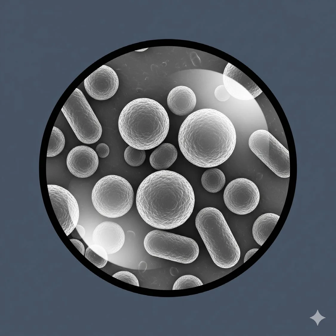
Surface morphology, size, shape and aggregation state of dried nanocarriers.
Purpose
To visualise the surface morphology, size, shape and aggregation state of nanocarriers at high resolution (typically 1–20 nm). Ideal for observing dried nanoparticle samples on a substrate.
Principle
A focused beam of electrons scans the sample surface. Secondary electrons emitted from the surface are detected to generate a 3D-like topographical image.
Standard protocol
- 1
Sample preparation
- Dilute the nanoparticle suspension in water or buffer (e.g., 1:10).
- Deposit 5–10 μL of sample onto a clean glass coverslip or conductive stub.
- Let it air-dry in a dust-free environment (or under a gentle nitrogen stream).
- 2
Washing (optional)
- Rinse gently with deionised water or ethanol to remove salts or excess reagent.
- Air-dry again.
- 3
Mounting
- Attach the sample to a metal stub using conductive tape or paint.
- 4
Coating (essential for non-conductive samples)
- Sputter-coat with a thin layer (~5–15 nm) of gold/palladium or carbon to prevent charging.
- 5
Imaging
- Load the sample into the SEM chamber under vacuum.
- Set accelerating voltage to 5–15 kV (lower for sensitive organic materials).
- Adjust working distance and focus.
- Capture images at various magnifications (e.g., 10k×, 50k×, 100k×).
- 6
Analysis
- Measure particle size and morphology (spherical, rod-like, aggregated).
- Assess sample homogeneity.
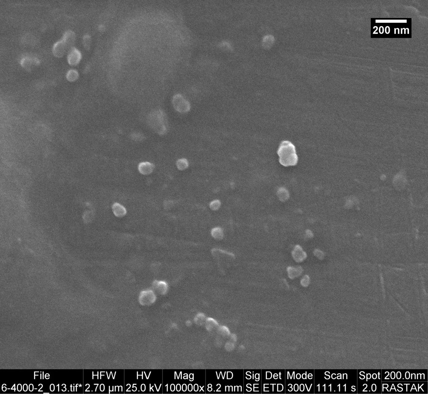
Representative data
Let's engineer the next delivery breakthrough together
We co-develop nanocarrier and biosensing programs with pharma, biotech and academic groups — from target selection through GMP supply.