
Microscopy & Microanalysis
SEM-EDS (Energy-Dispersive X-ray Spectroscopy)
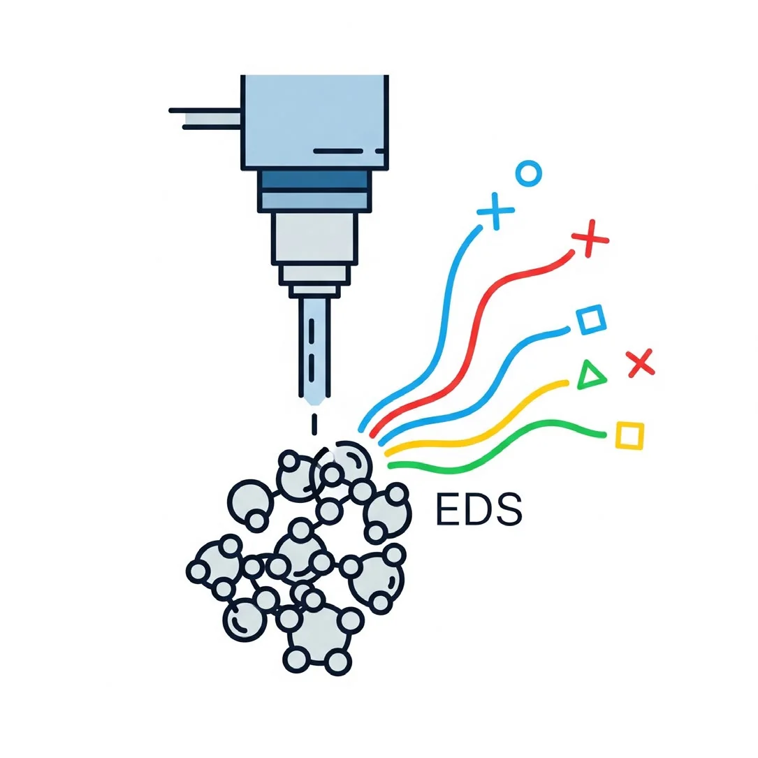
Elemental composition and mapping — confirming P, N, Si or metals in a carrier.
Purpose
To determine the elemental composition of a sample at specific locations. Useful for confirming the presence of key elements in nanocarriers (e.g., P from nucleic acids, N from cationic lipids, or Si from coatings).
Principle
When the electron beam hits the sample, it emits characteristic X-rays. EDS detects these X-rays to identify and quantify the elements present (typically Z ≥ 5, e.g., C, N, O, P, S, metals).
Standard protocol
- 1
Prepare sample
- Follow SEM sample preparation (coated, dried, mounted).
- 2
Locate region of interest (ROI)
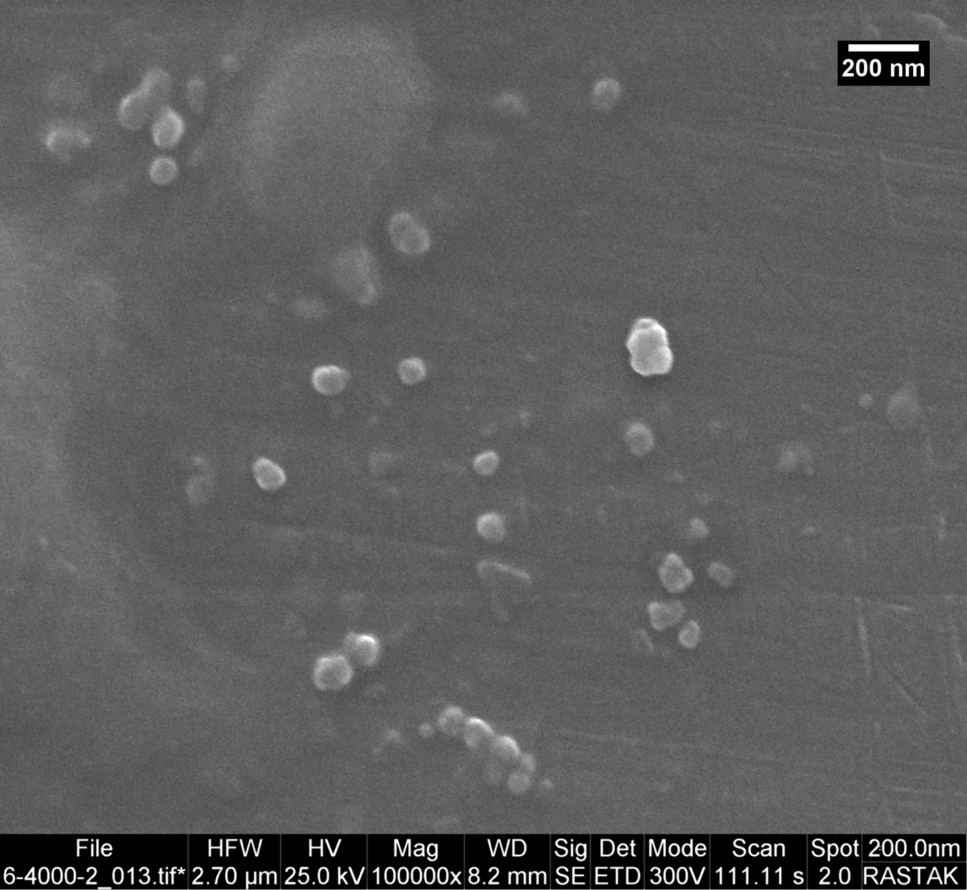
- Use SEM imaging to identify nanoparticles or aggregates.
- 3
EDS setup
- Set accelerating voltage to 10–20 kV (higher improves X-ray yield).
- Ensure working distance is optimised for EDS.
- 4
Acquisition
- Focus on the ROI.
- Start the EDS scan (live time: 30–100 seconds).
- Collect the X-ray spectrum.
- 5
Analysis
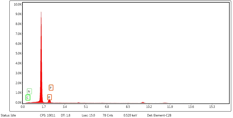
- Identify peaks corresponding to elements (e.g., P at ~2.0 keV for phosphate in DNA/RNA, N at ~0.4 keV).
- Perform semi-quantitative analysis (weight % or atomic %).
- Map elemental distribution (optional): create spatial maps of C, N, O, P, etc.
Representative data
Let's engineer the next delivery breakthrough together
We co-develop nanocarrier and biosensing programs with pharma, biotech and academic groups — from target selection through GMP supply.